CTS w/TritonCTS and Signal Integrity
CTS H-Tree
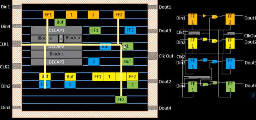
In the first image figure above, the CLK port connects to the clock pins of various flip-flops, based on connectivity information. However, in this example, the connections were made without considering physical factors — resulting in a situation where , meaning the clock arrives later at one flip-flop than the other.
This difference in arrival time is called clock skew.
Clock Skew
Clock skew is the variation in arrival times of the clock signal at different points within a synchronous system. More specifically, it is the difference in propagation delay of the clock signal as it travels through different paths to reach flip-flops.
Skew can be caused by:
- Differences in wire lengths
- Variations in routing paths
- Uneven buffer insertion delays
- Physical and environmental factors (temperature, voltage, etc.)
As a result, some parts of the circuit may receive the clock earlier or later than others — potentially leading to timing violations such as setup or hold failures.
Ideally, the skew should be as close to zero as possible.
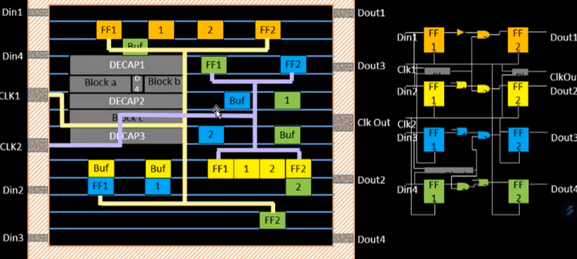
In the diagram, the clock tree is poorly constructed — the skew is significant due to unbalanced routing. This makes it a bad clock tree, as it undermines the core requirement of synchronous design: that all flip-flops receive the clock at nearly the same time.
Optimizing with H-Tree Routing
One common solution to balance skew is H-Tree routing. This method works as follows:
- Calculate the geometric center (midpoint) between all clock endpoints.
- Route the clock to that midpoint, then recursively find midpoints of each segment.
- At each midpoint, split the wire symmetrically.
- Repeat until the signal reaches all flip-flops.
The result is a symmetrical, balanced tree, where the clock travels equal distances to each destination — minimizing skew.
Signal Integrity and Buffer Insertion
While H-Tree routing balances delays, the clock signal can still degrade due to resistance and capacitance in long wires — causing distortion or attenuation.
To address this, clock buffers (repeaters) are inserted at regular intervals to:
- Restore signal strength
- Maintain sharp transitions
- Preserve timing integrity
Clock vs Data Buffers: Key Differences
- Clock Buffers: Designed with equal rise and fall times to maintain symmetric timing across the clock network — essential for predictable timing closure.
- Data Buffers: Rise and fall times may differ depending on signal conditions, load, and logic behavior. The emphasis here is on functional correctness rather than perfect symmetry.