Cell Design
Inputs for Standard Cell Design Flow
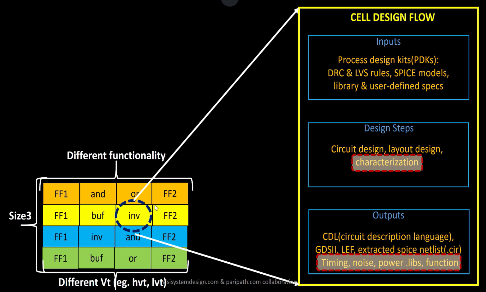
A standard cell (like an AND gate, OR gate, buffer, etc.) is a reusable, pre-characterized building block for digital ICs. These cells are stored in a standard cell library, which provides multiple versions of each cell — varying by drive strength, threshold voltage , and size. Larger cells have higher drive strength to handle longer wires or larger loads, while low- cells switch faster but may leak more power.
Key inputs for designing a standard cell library:
- PDKs (Process Design Kits)
- DRC (Design Rule Check) & LVS (Layout Versus Schematic) rules: Define fabrication constraints, minimum feature sizes, metal spacing, poly layers, well taps, etc.
- Tech files: Define layers, masks, and process-specific parameters.
- SPICE Models
- Transistor-level models for NMOS and PMOS devices.
- Include equations for threshold voltage, saturation, and linear regions, plus foundry-specific parameters for accurate simulation.
- User-Defined Specs
- Target cell height and width (fits the standard cell row grid).
- Supply voltage , pin locations, metal layer usage.
- Design goals for power, speed, and noise margin.
Processes: Circuit, Layout & Characterization
The standard cell design flow turns these inputs into manufacturable, reusable cells:
- Circuit Design
- Transistor-level schematics are created using NMOS and PMOS models.
- Sizing is optimized to meet performance, power, and fan-out requirements.
- Layout Design
- Physical layout is drawn based on the schematic.
- Techniques like Euler paths and stick diagrams help create compact, efficient transistor arrangements.
- Tools like Magic, Cadence Virtuoso, or Synopsys Custom Compiler are commonly used.
- Characterization
- Cells are simulated using SPICE to extract real-world timing, power, and noise data. Output files are generated for use by EDA tools during synthesis and place-and-route. The finished cell netlists and SPICE models are given to characterization software (such as GUNA) through a configuration file. This flow typically includes:
- Reading SPICE model files
- Reading the netlist extracted from the schematic/layout
- Recognizing circuit behavior (e.g., buffer or gate type)
- Reading subcircuits and connecting power sources
- Applying input stimulus (test vectors)
- Adding output capacitance to model real loading conditions
- Running SPICE simulations with proper commands
- The output is a set of .lib files describing timing, noise, and power — these are essential for synthesis, static timing analysis, and physical design.
- Cells are simulated using SPICE to extract real-world timing, power, and noise data. Output files are generated for use by EDA tools during synthesis and place-and-route. The finished cell netlists and SPICE models are given to characterization software (such as GUNA) through a configuration file. This flow typically includes:
Outputs: What the Library Provides
A finished standard cell library includes:
- Circuit Description: Schematic netlist (e.g., in CDL format)
- Layout Data: GDSII (geometry), LEF (abstract physical data)
- Timing and Noise Models: Liberty (.lib) files for synthesis and static timing analysis
- Parasitic Data: Resistance, capacitance, and noise behavior for accurate post-layout simulation.
The entire cell design must strictly follow foundry DRC and LVS rules — any violations can cause the cell to fail manufacturing checks or introduce errors when integrated in a real chip.